High Productivity UBM/RDL
Introduction
With the drive for improved performance and smaller form factor, packaging schemes based on wafer bumping rather than traditional wire-bond are becoming the default for new designs. PVD systems are used to deposit Under Bump Metallization (UBM) layers to enable bump metals to adhere to die electrical pad contacts, or to act as seeds for Cu plated Re-Distribution Layers (RDL).
Issues with Organics
PI or PBO used as re-passivation in UBM/RDL, adhesives for thinned Si mounted on carriers in 2.5D/3D-IC process flows and epoxy mold compound substrates used in Fan-Out WLP applications are examples of organic materials encountered in advanced packaging schemes
Organics are well-known to absorb contamination such as moisture, which affects subsequent PVD processes and film quality. Removal of such contaminants prior to UBM/RDL metal deposition is critical to maximising yield, particularly with shrinking device designs where reduced CDs are more sensitive to contamination. As moisture content is reduced, contact resistance (Rc) improves (see Fig 1).
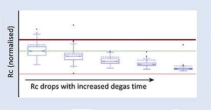
Fig 1 Benefit of increasing degas time - Reduced Rc
Traditional PVD systems used in FEOL processing remove moisture and other contaminants by heating wafers to high temperatures (typically > 300°C) for a short period of time in a single wafer processing chamber prior to metal deposition. Processes are relatively short, but effective, as high temperatures can be used with the inorganic materials involved.
The use of organic materials in packaging schemes however presents challenges for PVD. Organics tend to have low thermal budget, as low as 120°C in some cases. To maintain effective contamination removal, wafers require extended degas times at lower temperatures.
With a single wafer process chamber concept for wafer degas, system throughputs reduce as degas time increases and cost per wafer increases as a result.
High Throughput at Low Temperature
The SPTS Sigma® fxP PVD system uses a novel degas chamber design to overcome this issue. The MWD (Multi-Wafer Degas) module is based on a batch rather than single wafer concept. Using this approach there is always a clean wafer available to process, eliminating degas as a throughput bottleneck. Wafers dynamically pumped under clean, high vacuum conditions, with radiation heat transfer warming wafers directly to temperatures within the operating regimes for packaging applications.
A Sigma® fxP configured with MWD will deliver throughputs > 1.5x competitor UBM systems based on single wafer degas processing technology. As new materials emerge with even lower thermal budgets, longer degas times can be employed with no impact on throughput (See Fig 2). Conversely, competitor systems based on single wafer degas will get progressively slower.
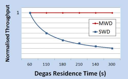
Fig 2 Longer Degas times - No impact on throughput with MWD
SPTS's MWD technology is production-proven with installations at several leading OSATs, used for UBM/RDL processing of leading edge technology node devices and for Fan-Out WLP products.
